
FPGAs in embedded systems
A gate array is a digital integrated circuit containing a large number of logic elements that can be connected in an arbitrary manner to form complex digital devices. Many FPGAs even support the implementation of a full-blown microcontroller together with an array of I/O devices. A microcontroller or microprocessor implemented using the gates of an FPGA is referred to as a soft processor.
Early versions of gate arrays were one-time programmable devices in which a circuit design would be implemented within a device at the factory where the device was constructed, or perhaps by system developers using a programming device connected to their desktop computers. Once a device had been programmed, it could not be changed. Since that time, the technology of gate arrays has improved and now reprogrammable gate arrays are widely available.
Today, there is a tremendous variety of Field-Programmable Gate Arrays (FPGAs) available even to system developers of modest means. As the name implies, FPGAs are gate arrays that can be reprogrammed at any time, even after an embedded system has been assembled and delivered to its end user.
Before we get into the specifics of FPGA devices, we'll introduce some underlying concepts related to digital circuits, specifically logic gates and flip-flops.
Digital logic gates
A modern FPGA device contains what we might think of as a large box of digital parts that can be used to assemble complex logic circuits. The simplest of these components include the AND, OR, and XOR gates that perform basic logic functions. Each of these gates has two inputs and one output. The NOT gate is even simpler, with one input and one output. Logic gates operate on the binary input values 0 and 1 and produce an output of 0 or 1 as determined by the inputs.
In reality, the binary values in these circuits are represented by a voltage, with 0 usually represented as a low voltage (near zero volts) and 1 as a higher voltage that depends on the technology of the circuitry in which the gates are implemented. A common level for the 1 value in modern circuitry is 3.3 volts.
We will briefly discuss the behavior of each of these gates and present the gate's schematic symbol and the truth table that defines the gate's behavior. The behavior of a logic gate can be represented as a truth table where, for each possible combination of inputs, the output is given. Each column represents one input or output signal, with the output shown at the right side of the table. Each row presents one set of input values with the output of the gate given those inputs.
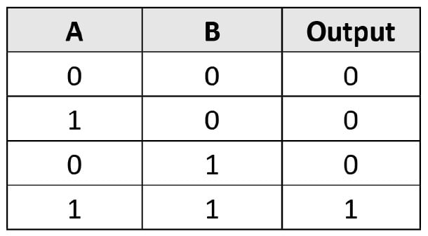
The AND gate outputs a 1 when both of its inputs are 1, otherwise the output is 0. Figure 1.3 is the AND gate schematic symbol:
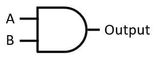
Figure 1.3 – AND gate schematic symbol
The following table is the truth table for the AND gate:
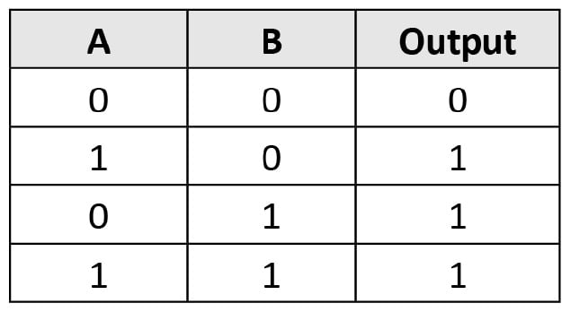
The OR gate outputs a 1 if either of its inputs is 1, otherwise the output is 0. Figure 1.4 is the OR gate schematic symbol:
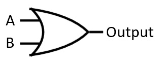
Figure 1.4 – OR gate schematic symbol
The following table is the truth table for the OR gate:
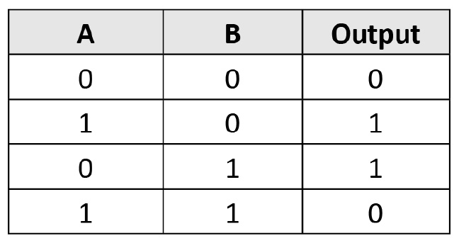
The XOR gate outputs a 1 if exactly one of its outputs is 1, otherwise the output is 0. Figure 1.5 is the XOR gate schematic symbol:
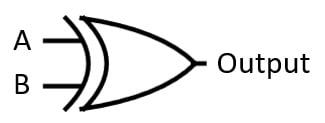
Figure 1.5 – XOR gate schematic symbol
The following table is the truth table for the XOR gate:
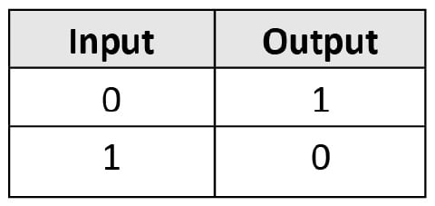
The NOT gate has a single input and an output that is the inverse of its input: An input of 0 produces an output of 1, and an input of 1 produces an output of 0. Figure 1.6 is the NOT gate schematic symbol:
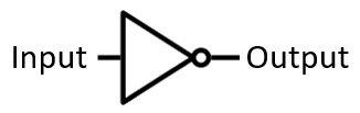
Figure 1.6 – NOT gate schematic symbol
In Figure 1.6, the triangle represents an amplifier, meaning this is a device that turns a weaker input signal into a stronger output signal. The circle represents the inversion operation.
The following table is the truth table for the NOT gate:
Each of the AND, OR, and XOR gates can be implemented with an inverting output. The function of an inverting gate is the same as described, except the output is the opposite of the output from the non-inverting gate. The schematic symbol for an AND, OR, or XOR gate with inverted output has a small circle added at the output side of the symbol, just as on the output of the NOT gate. The names of the gates with inverted outputs are NAND, NOR, and XNOR. The letter N in each of these names indicates NOT. For example, NAND means NOT AND, which is functionally equivalent to an AND gate followed by a NOT gate.
Flip-flops
A device that changes its output state only when a clock signal makes a specified transition (either low-to-high or high-to-low) is referred to as an edge-sensitive device. A flip-flop is an edge-sensitive device that holds one bit of data as its output signal. The flip-flop updates the data value it contains based on the state of its input signal when the clock input receives the specified transition.
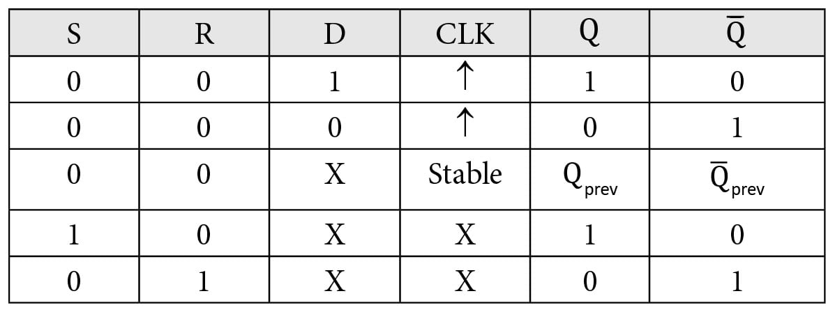
The positive edge-triggered D flip-flop is a common digital circuit component that finds use in a variety of applications. The D flip-flop typically includes set and reset input signals that force the stored value to 1 (set) or to 0 (reset). This type of flip-flop has a data input called the D input.
The D flip-flop has a clock input that triggers the transfer of the D input to the Q output on the clock's rising edge. The  output (the overbar here means NOT) always has the opposite binary value from the Q output. Other than within an extremely narrow window of time surrounding the rising edge of the clock signal, the flip-flop does not respond to the value of the D input. When active (at the 1 level), the S (set) and R (reset) inputs override any activity on the D and clock inputs.
Figure 1.7 shows the schematic symbol for the D flip-flop. The clock input is indicated by the small triangle on the left side of the symbol:
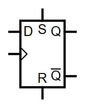
Figure 1.7 – D flip-flop
The truth table for the D flip flop is shown below. The upward-pointing arrows in the CLK column indicate the rising edge of the clock signal. The  and
and  outputs on the table rows containing upward-pointing arrows in the
 CLK column represent the state of the outputs following the rising clock edge. In this table, the value X indicates don't care, meaning it does not matter what value that signal has in determining the Q output. The output Qprev prev represents the most recent value of produced through the action of the S, R, D, and CLK inputs:
Any digital circuit composed of a collection of logic gates is referred to as combinational logic when the output at any moment depends only on the current state of the inputs. In other words, the output does not depend on previous input values. Combinational logic circuits have no memory of past inputs or outputs.
Armed with this background information on logic gates and flip-flops, we will next discuss the implementation of circuits composed of these and related components in FPGAs.
Elements of FPGAs
The digital parts available within an FPGA typically fall into the categories of lookup tables, flip-flops, block RAM, and DSP slices. We will briefly examine each of these components.
Lookup tables
Lookup tables are used extensively in FPGAs to implement combinational logic circuits constructed from simple logic gates such as NOT, AND, OR, and XOR, as well as the siblings of the last three of these with inverted outputs: NAND, NOR, and XNOR.
Rather than implementing a logic gate circuit in hardware with the actual gates in its design, it is always possible to represent the same circuit using a simple lookup table. Given any combination of input signals, the correct output can be retrieved from a memory circuit addressed by the inputs. A typical FPGA lookup table has six single-bit input signals and a single bit output. This is equivalent to a single-bit-wide memory device with six address inputs holding 64 bits of data (26 = 64). Circuits that require fewer than six inputs can treat some of the inputs as don't care inputs. Circuits with greater complexity can combine multiple lookup tables to produce their results.
Flip-flops
For a digital circuit to retain any record of past events, some form of memory is required. As presented in the previous section, a flip-flop is a high-speed single-bit memory storage device. As with lookup tables, FPGAs contain large numbers of flip-flops to support the construction of complex sequential logic circuits. Digital circuitry that generates outputs based on a combination of current inputs and past inputs is called sequential logic. This is in contrast to combinational logic, where outputs depend only on the current state of the inputs.
Block RAM
A Block RAM (BRAM) is a range of dedicated memory locations within an FPGA. In comparison to traditional processor hardware, flip-flops can be likened to processor registers, while BRAM is more like cache memory. Cache memory in a processor is used to temporarily store copies of recently accessed memory contents in a memory area where the processor can access it again, if it needs to, much faster than reaching out to main memory. FPGA synthesis tools allocate BRAM to circuit designs in a manner that optimizes the performance of the digital circuit.
DSP slices
A DSP slice is a section of digital logic optimized to perform the central computation of digital signal processing – the Multiply-Accumulate (MAC) operation. MAC processing involves multiplying two lists of numbers element by element and adding the products together. As a simple example, if two sequences are defined as a0, a1, a2 and b0, b1, b2, the result of a MAC operation on these sequences is a0b0 + a1b1 + a2b2. Many DSP algorithms are built upon repetitive MAC operations performed with a list of algorithm-specific coefficients on a stream of input data.
Other functional elements
Every FPGA manufacturer expends significant effort to ensure each FPGA model provides the highest performance possible for use in a wide range of application areas. In order to better meet a diversity of needs, FPGAs often include hardware implementations of additional categories of low-level digital components such as shift registers, carry logic, and multiplexers. The inclusion of these hardware elements enables the synthesis of better-performing algorithms in comparison to an FPGA that generates these low-level components from the more generic resources available within the device.
The next section introduces the FPGA synthesis process, which converts a high-level description of an FPGA algorithm into a circuit implementation within a specific FPGA device.
FPGA synthesis
Although an FPGA device contains a large collection of low-level digital building blocks used to implement complex digital devices, it is important for system developers who are new to FPGA technology to understand that, in most cases, designers do not need to work directly at the level of these components. Instead, digital designers specify the system configuration as a combination of higher-level predefined functional blocks, such as a soft processor, and custom digital logic defined using a hardware description language. It is also possible to specify FPGA algorithms using programming languages such as C and C++.
The process of converting the high-level description of device functionality into the allocation and interconnection of the lookup tables, flip-flops, BRAM, and other device components is called FPGA synthesis. The synthesis process is conceptually similar to the software compilation process that converts human-readable source code to a binary program that can be executed by a processor.
Hardware design languages
It is easy to represent simple digital circuits using logic diagrams based on the schematic symbols presented earlier in this chapter. When designing digital devices that are very complex, however, the use of logic diagrams quickly becomes unwieldy. As an alternative to the logic diagram, a number of hardware description languages have been developed over the years.
The two most popular hardware design languages are VHDL and Verilog. VHDL is a multilevel acronym where the V stands for VHSIC, which means Very High-Speed Integrated Circuit, and VHDL stands for VHSIC Hardware Description Language. The syntax and some of the semantics of VHDL are based on the Ada programming language. Verilog has capabilities similar to VHDL. Although the two languages are not equivalent, it is broadly true that almost any digital design that you might implement in one of these languages can be implemented in the other language.
To provide a quick comparison between schematic diagram-based logic design and designing with a hardware description language, we will look at a simple adder circuit. A full adder adds two data bits plus an incoming carry bit and produces a one-bit sum and a carry output bit. This circuit, shown in Figure 1.8, is called a full adder because it includes the incoming carry in the calculation. A half adder, in comparison, adds only the two data bits without an incoming carry:
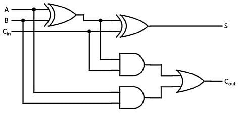
Figure 1.8 – Full adder circuit
The full adder uses logic gates to produce its output as follows: The sum bit S is 1 only if the total number of 1 bits in the collection A, B, Cin is an odd number. Otherwise, S is 0. The two XOR gates perform this logical operation. Cout is 1 if both A and B are 1, or if just one of A and B is 1 and Cin is also 1. Otherwise, Cout is 0.
The VHDL code in the following listing defines a digital circuit that performs the equivalent full adder function:
-- Load the standard libraries

library IEEE;
  use IEEE.STD_LOGIC_1164.ALL;

-- Define the full adder inputs and outputs

entity FULL_ADDER is
  port (
    A     : in    std_logic;
    B     : in    std_logic;
    C_IN  : in    std_logic;
    S     : out   std_logic;
    C_OUT : out   std_logic
  );
end entity FULL_ADDER;

-- Define the behavior of the full adder

architecture BEHAVIORAL of FULL_ADDER is

begin

  S     <= (A XOR B) XOR C_IN;
  C_OUT <= (A AND B) OR ((A XOR B) AND C_IN);

end architecture BEHAVIORAL;
This code is a fairly straightforward textual description of the full adder in Figure 1.8. Here, the section introduced with entity FULL_ADDER is defines the input and output signals of the full adder component. The architecture section toward the end of the code describes how the circuit logic operates to produce the outputs S and C_OUT given the inputs A, B, and C_IN. The term std_logic refers to a single-bit binary data type. The <= characters represent wire-like connections that drive the output on the left-hand side with the value computed on the right-hand side.
It is important, especially for FPGA developers coming from a software background, to understand that there is no concept of sequential execution in VHDL code. The statements in the BEHAVIORAL section at the end of the code that associate the outputs S and C_OUT with logical expressions are defining a digital circuit equivalent to Figure 1.8. They are not specifying computations that execute in sequence as in a traditional software program.
The benefits of using FPGAs in embedded system designs
For embedded system architects who are new to developing with FPGAs, the many benefits of using these devices may not be immediately obvious. Although FPGAs certainly are not appropriate for every embedded system design, it is useful to consider whether the use of FPGA technology is appropriate for your next system design.
Some of the benefits of developing embedded systems with FPGAs are as follows:
- Processor customization: Because the soft processors used in FPGAs are programmed into the device, it is standard for the developers of these products to provide a variety of configuration alternatives to the end user. Some common options are a choice between a 64-bit or 32-bit processor, the inclusion or exclusion of a floating-point processor, and the inclusion or exclusion of instructions that require significant hardware resources, such as integer division. These are just a few of the options that are likely to be available. The soft processor configuration can be modified even late in the development cycle to optimize trade-offs between system performance and FPGA resource utilization.
- Flexible peripheral configuration: Since the I/O interfaces in an FPGA design are defined in software, designers can include exactly the I/O devices they need and avoid including I/O hardware they don't need. As with processor customization, it is straightforward to modify the types and the number of I/O devices even late in the development cycle.
- High-level synthesis: Modern FPGA development tools support the definition of computationally intensive algorithms in traditional programming languages, including C and C++. This allows system developers with a software skill set to develop algorithms in a traditional software development environment and directly transition the same code into an optimized FPGA implementation. The FPGA version of the algorithm is relieved of traditional processor-based restrictions, such as sequential instruction execution and a fixed memory architecture. The high-level synthesis tools will generate an FPGA implementation that exploits execution parallelization and defines a memory architecture best suited to the algorithm. A custom hardware algorithm can be combined with a soft processor to implement a complete, high-performance digital system on a single FPGA device.
- Hardware acceleration for parallelizable applications: Any algorithm that benefits from parallelization is a candidate for implementation as custom FPGA logic. Rather than executing an algorithm sequentially with processor instructions, FPGA hardware can often perform the processing in parallel much faster. Many modern FPGA devices contain dedicated hardware to support digital signal processing (DSP) operations. These capabilities are available for use by many types of parallel algorithms, such as digital filtering and neural networks.
- Extensive debugging capabilities: Soft processors often provide options to enable a variety of debugging capabilities, such as instruction tracing, multiple complex breakpoints, and the ability to monitor the innermost operations of the processor and its interactions with other system components at the hardware level. As system development wraps up, developers can remove resource-intensive debugging capabilities from the final design to enable deployment in a smaller and less costly FPGA device.
- Rapid prototyping of ASIC designs: For embedded system designs intended to support the high volume that makes ASIC usage cost-effective, it is helpful to perform early prototyping with FPGAs to validate the system's digital design prior to investing in an ASIC implementation. The use of FPGAs in this context enables rapid development iterations that enable extensive testing of the new features introduced at each build iteration.
Xilinx FPGAs and development tools
There are several manufacturers of FPGA devices and the development tools associated with them. To avoid trying to cover multiple vendors and their FPGA devices and development toolchains, and to avoid discussing these topics at too abstract a level, we are going to select one vendor and one set of development tools for use in the examples and projects developed in this book. This is not to suggest that another vendor's devices and tools aren't as good, or possibly better, for the applications we will discuss. We are simply choosing to use Xilinx FPGA devices and development tools to make the steps we are taking concrete and to allow you to follow along.
The Vivado Design Suite is available as a free download from Xilinx, though you will need to create a Xilinx user account to access the download page. Visit https://www.xilinx.com/ and select the option to create your account. Once you are logged in on the website, visit https://www.xilinx.com/support/download.html and download the Vivado Design Suite.
Vivado can be installed on Windows and Linux operating systems. Our projects in the coming chapters can be developed with Vivado running under either operating system.
Vivado includes a set of simulation capabilities that will allow you to develop and execute FPGA implementations within the simulation environment at zero cost. When you decide you need to see your FPGA design run on an actual FPGA, the best option for the projects we will be covering is the Arty A7-100T. This board currently costs US$249 and is available at https://store.digilentinc.com/arty-a7-artix-7-fpga-development-board-for-makers-and-hobbyists/.