
Introducing FPGAs
A gate array in ASIC terms is a sea of gates with some number of mask steps that can be configured for a given application. This allows for a more inexpensive product since the company designing the ASIC only needs to pay for the masks necessary for configuring. The FPGA takes this one step further by providing the programmability of the fabric as part of the device. This does result in an increased cost as you are paying for interconnect you are not using and the storage devices necessary to configure the FPGA fabric, but allows for some cost reductions as these parts become standard devices that can be mass produced.
If we look at the functions in the previous section through the adder example, we can see one commonality; they can all be produced using a truth table. This becomes key in FPGA development. We can regard these truth tables as Read Only Memory (ROM) representations of the functions. In fact, we can regard them as Programmable ROMs (PROMs) in the case of building up our FPGA.
Let's take the example of the fundamental logic functions. We can reproduce any of them by utilizing a 2-input lookup table, which could look something like this:
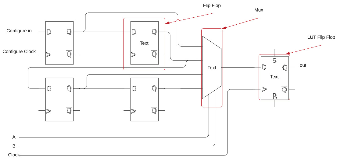
Figure 1.7 – Two input LUT examples
This is an oversimplified example, but what we have are four storage elements, in this case flip-flops, but in the case of an actual FPGA, more likely a much simpler structure utilizing far fewer transistors. The storage elements are connected to one another such that their configuration can be loaded. By attaching other Lookup Tables (LUTs) to the chain, multiple LUTs can be configured at startup, or in the case of partial reconfiguration, during normal operation. By adding a flip-flop, we can see the final structure of the LUT take shape.
The power in the simplicity of the structure is the ability to replicate this design many times over. In the case of modern FPGAs, they are built of many tiles or columns of logic such as this, allowing a much simpler piece to be designed, implemented, and verified, and then replicated to produce the large gate count devices available. This allows for a range of lower cost devices with fewer columns of resources to larger devices with many more, some even using Stacked Silicon Interconnects (SSI), which allows multiple ASIC dies to be attached together via an interconnect substrate.
In 1985, Xilinx introduced the XC2064, what we would consider the first FPGA utilizing an array of 64 3-input LUTs with one flip-flop. The breakthrough with this design was that it was modular and had good interconnect resources. This entire part would be approximately equivalent to 1 Combination Logic Block (CLB) in the Artix-7 we will be targeting.
At the heart of an FPGA is the programmable fabric. The fabric consists of LUTs with associated flip-flops making up slices and ultimately CLBs. These blocks are all connected using a rich topology of routing channels, allowing for almost limitless configuration. FPGAs also contain many other resources that we will explore over the course of this book, block RAMs, Serial-Deserial (SERDES) cores, DSP elements, and many types of programmable I/O.
Exploring the Xilinx Artix-7 and 7 series devices
The FPGAs we will be looking at in this book are the Artix-7 series of devices. These devices are the highest performance per watt of the Xilinx 7 series devices. For a reasonable price, they feature a large amount of relatively high-performance logic to implement your designs. The FPGA components we will introduce here are common in the Spartan (low end), Kintex (mid-range) and Virtex (high end) parts in the 7 series.
Combinational logic blocks
ASICs are made up of logic gates based upon libraries provided by ASIC foundries, such as TSMC or Tower. These libraries can contain everything from AND, OR, and NOT gates to more complicated math cells and storage elements. When developing an FPGA, you will be targeting the same Boolean logic equations as you would in an ASIC. We will be using a very similar flow. However, the synthesis process will target the CLBs of the FPGA:
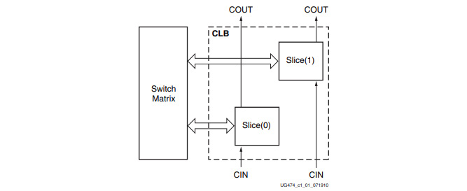
Figure 1.8 – Xilinx UG474 7 series FPGAs CLB users' guide figure 1-1 (used with permission)
A CLB consists of a pair of slices, each of which contains four 6-input LUTs and their eight flip-flops. Vivado (or optionally a third-party synthesis tool such as Synopsys Synplify) compiles the SystemVerilog code and maps it to these CLB elements. To fully explore the details of the CLB, I would suggest reading Xilinx UG474, 7 Series FPGAs CLB users' guide (https://www.xilinx.com/support/documentation/user_guides/ug474_7Series_CLB.pdf). At a high level, each LUT allows a degree of flexibility such that any Boolean function with 6 inputs can be implemented or two arbitrarily defined 5-input functions if they share common inputs. There is also dedicated high speed carry logic for arithmetic functions, which will be discussed in later chapters.
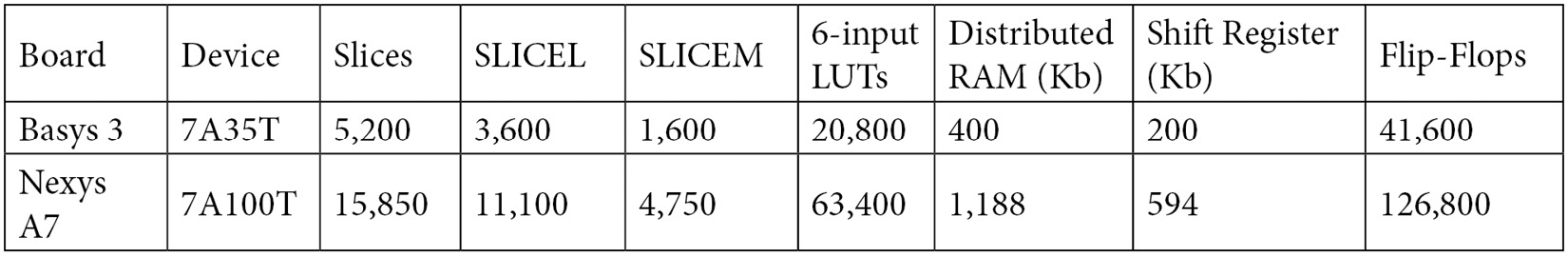
The slices come in two formats, SLICEL (logic) and SLICEM (memory). SLICEM is a superset of SLICEL. SLICEM adds the ability to configure the SLICE into a distributed RAM or shift register. There are approximately three times the number of SLICELs as SLICEMs. The following table for the two suggested development boards for this book shows the breakdown:
Although it is theoretically possible to instantiate and force the functionality of lower-level components, such as slices or LUTs, this is beyond the scope of this book, and a feature not widely used. We will be targeting CLB usage through Vivado synthesis of the HDL that we write.
Storage
Aside from the SLICEMs that make up the CLBs that can be used as memories or shift registers, FPGAs contain Block RAMs (BRAM) that are larger storage elements. The 7 series parts all have 36 Kb BRAM that can be split into two 18 Kb BRAMs. The following table shows the BRAM available in the parts on the recommended development boards:

BRAMs can be configured as follows:
- True dual port memories – Two read/write ports.
- Simple dual port memories – 1 read/1 write. In this case, a 36 Kb BRAM can be up to 72 bits wide and an 18 Kb BRAM up to 36 bits wide.
- A single port.
Contents of BRAMs can be loaded at initialization and configured via a file or initial block in the code. This can be useful for implementing ROMs or start up conditions.
BRAMs in 7 series devices also contain logic to implement FIFOs. This saves CLB resources and reduces synthesis overhead and potential timing problems in a design. We will go over FIFOs in a later chapter.
All 36 Kb BRAMs have dedicated Error Correction Code (ECC) functions. As this is something more related to high reliability applications, such as medical-, automotive-, or space-based, something we will not go into detail on in this book.
Clocking
7 series devices implement a rich clocking methodology, which can be explored in detail in UG472 7 Series FPGAs clocking resources user guide (https://www.xilinx.com/support/documentation/user_guides/ug472_7Series_Clocking.pdf). For most purposes, our discussion in the PLL section will give you everything you need to know; however, the referenced document will delve into far more detail.
I/Os
For the most part, we will limit ourselves to the I/Os supported by the two targeted development boards. In general, the 7 series devices handle a variety of interfaces from 3.3v CMOS/TTL to LVDS and memory interface types. The boards we are using will dictate the I/Os defined in our project files. For more information on all the supported types, you can reference the UG471 7 Series FPGAs SelectIO resources user guide.
DSP48E1
FPGAs have a large footprint in Digital Signal Processing (DSP) applications that use a lot of multipliers and, more specifically, Multiply Accumulate (MAC) functions. One of the first innovations in FPGAs was to include hard multipliers followed by DSP blocks that could implement MAC functions:
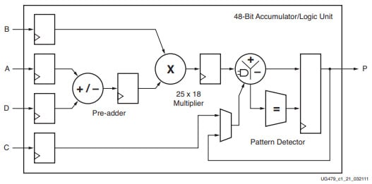
Figure 1.9 – Xilinx UG479 7 series DSP48E1 users' guide figure 1-1 (used with permission)
One of the most expensive operations in an FPGA is arithmetic. In an ASIC, the largest and slowest operation is typically a multiplication operation, and the smaller or faster operation is an add operation. For this reason, for many years, FPGA manufacturers have been implementing hard arithmetic cores in their fabric. This makes the opposite true in an FPGA, where the slower operation is typically an adder, especially as the widths get larger. The reason for this is that the multiply has been hardened into a complex, pipelined operation. We will explore the DSP operator more in later chapters. The UG479 7 Series DSP48E1 user guide (https://www.xilinx.com/support/documentation/user_guides/ug479_7Series_DSP48E1.pdf) is a good reference if you are interested in delving into the details.